Purpose
The RT2855BH is an Advanced Constant On-Time (ACOT™) control architecture step-down converter with the input voltage range from 4.5V to 18V and provides 4A output current. This document explains the function and use of the RT2855BH evaluation board (EVB), and provides information to enable operation, modification of the evaluation board and circuit to suit individual requirements.
Introduction
General Product Information
The RT2855BH is a high-performance 650kHz 4A step-down regulator with internal power switches and synchronous rectifiers. It features quick transient response using its Advanced Constant On-Time (ACOT™) control architecture that provides stable operation with small ceramic output capacitors and without complicated external compensation, among other benefits. The input voltage range is from 4.5V to 18V and the output is adjustable from 0.765V to 7V.
Product Feature
-
Fast Transient Response
-
Steady 650kHz Switching Frequency at all Load
-
4A Output Current
-
Advanced Constant On-Time (ACOT™) Control
-
Optimized for Ceramic Output Capacitors
-
4.5V to 18V Input Voltage Range
-
Internal 70mΩ Switch and 30mΩ Synchronous Rectifier
-
0.765V to 7V Adjustable Output Voltage
-
Externally-adjustable, Pre-biased Compatible Soft-Start
-
Cycle-by-Cycle Current Limit
-
Optional Output Discharge Function
-
Output Over- and Under-voltage Shut-down in Hiccup Mode
-
Input Under Voltage Lockout
-
Thermal Shutdown
Key Performance Summary Table
|
Key Features
|
Evaluation Board Number : PCB023_V1
|
|
Default Input Voltage
|
12V
|
|
Max Output Current
|
4A
|
|
Default Output Voltage
|
1.05V
|
|
Default Marking & Package Type
|
RT2855BHGQW, WQFN-16 3x3
|
Bench Test Setup Conditions
Headers Description and Placement
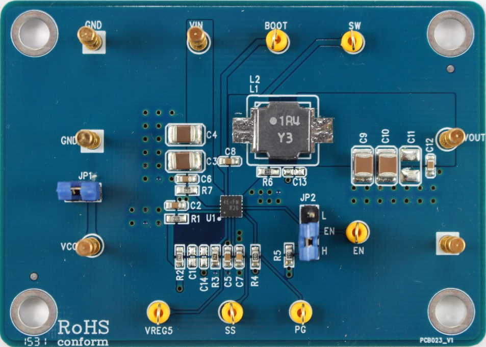
Please carefully inspect the EVB IC and external components, comparing them to the following Bill of Materials, to ensure that all components are installed and undamaged. If any components are missing or damaged during transportation, please contact the distributor or send e-mail to evb_service@richtek.com
Test Points
The EVB is provided with the test points and pin names listed in the table below.
|
Test point/
Pin name
|
Signal
|
Comment (expected waveforms or voltage levels on test points)
|
|
VIN
|
Input voltage
|
Power input. Support 4.5V to18V Input Voltage. Must bypass with a suitable large ceramic capacitor at this pin.
|
|
EN
|
Enable test point
|
A logic-high enables the converter; a logic-low forces the IC into shutdown mode reducing the supply current to less than 10µA.
|
|
GND
|
Ground
|
Ground.
|
|
VCC
|
Internal regulator output
|
VCC supplies power for the internal linear regulator that powers the IC. Connect VIN to the input voltage and bypass to ground with a 0.1µF ceramic capacitor.
|
|
BOOT
|
Bootstrap supply test point
|
Bootstrap supply for high-side gate driver. Connect a 0.1µF capacitor
between BOOT and SW to power the internal gate driver.
|
|
SW
|
Switch node test point
|
SW is the source of the internal N-channel MOSFET switchand the drain of the internal N-channel MOSFET synchronous rectifier. Connect SW to the inductor with a wide short PCB trace and minimize its area to reduce EMI.
|
|
VREG5
|
Internal regulator
|
Connect a 1µF capacitor to GND to stabilize output voltage.
|
|
SS
|
Soft-start control
|
Connect an external capacitor between this pin and GND to set the soft-start time.
|
|
PG
|
Open drain power good output
|
PGOOD connects to PGND whenever VFB is less than 90% of its regulation threshold (typical).
|
Power-up & Measurement Procedure
1. Apply a 12V nominal input power supply (4.5V < VIN < 18V) to the VIN and GND terminals.
2. Connect JP1 to connect VIN to VCC. Set the jumper at JP2 to connect terminals 2 and 3, connecting EN to VCC to enable operation.
3. Verify the output voltage (approximately 1.05V) between VOUT and GND.
4. Connect an external load up to 4A to the VOUT and GND terminals and verify the output voltage and current.
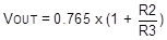
Output Voltage Setting
Set the output voltage with the resistive divider (R2, R3) between VOUT and GND with the midpoint connected to FB. The output is set by the following formula :
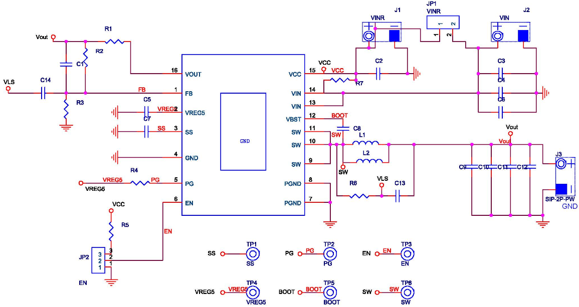
Schematic, Bill of Materials & Board Layout
EVB Schematic Diagram
Bill of Materials
|
Reference
|
Qty
|
Part Number
|
Description
|
Package
|
Manufacture
|
|
U4
|
1
|
RT2855BHGQW
|
DC/DC Converter
|
WQFN-16 3x3
|
RICHTEK
|
|
C1
|
1
|
|
NC
|
|
|
|
C2, C5, C6, C8, C12
|
5
|
C1608X7R1H104K080AA
|
0.1μF/±10%/50V/X7R
|
C-0603
|
TDK
|
|
C3, C4
|
2
|
UMK325BJ106MM
|
10µF/50V/X7R
|
C-1210
|
TAIYO YUDEN
|
|
C7
|
1
|
0603B332K500
|
3.3nF/50V/X7R
|
C-0603
|
WALSIN
|
|
C9
|
1
|
C3225X5R1E226MT
|
22µF/25V/X5R
|
C-1210
|
TDK
|
|
C10
|
1
|
C3225X5R1E226MT
|
22µF/25V/X5R
|
C-1210
|
TDK
|
|
C13
|
1
|
|
NA
|
|
|
|
C14
|
1
|
|
NA
|
|
|
|
L1
|
1
|
NR8040T1R4N
|
1.4µH/7A
|
8 x 8 x 4.2 mm
|
TAIYO YUDEN
|
|
R1
|
1
|
|
0
|
R-0603
|
|
|
R2
|
1
|
|
8.25k
|
R-0603
|
|
|
R3
|
1
|
|
22.1k
|
R-0603
|
|
|
R4, R5
|
2
|
|
100k
|
R-0603
|
|
|
R6, R7
|
2
|
|
NA
|
|
|
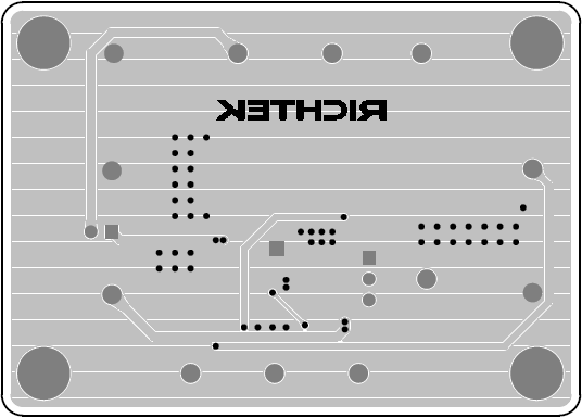
PCB Layout
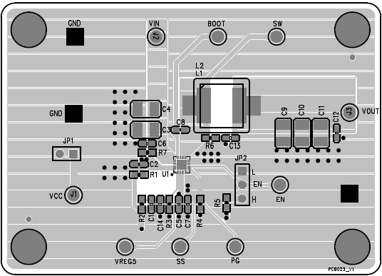
Top View (1st layer)
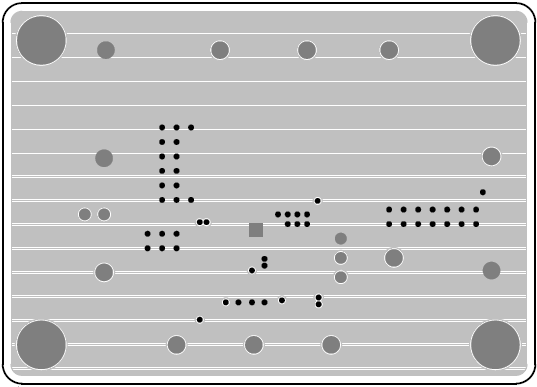
PCB Layout—Inner Side (2nd Layer)
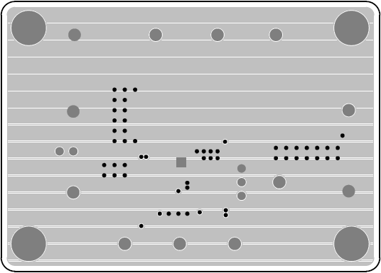
PCB Layout—Inner Side (3rd Layer)
Bottom View (4th Layer)